ABSRACT:
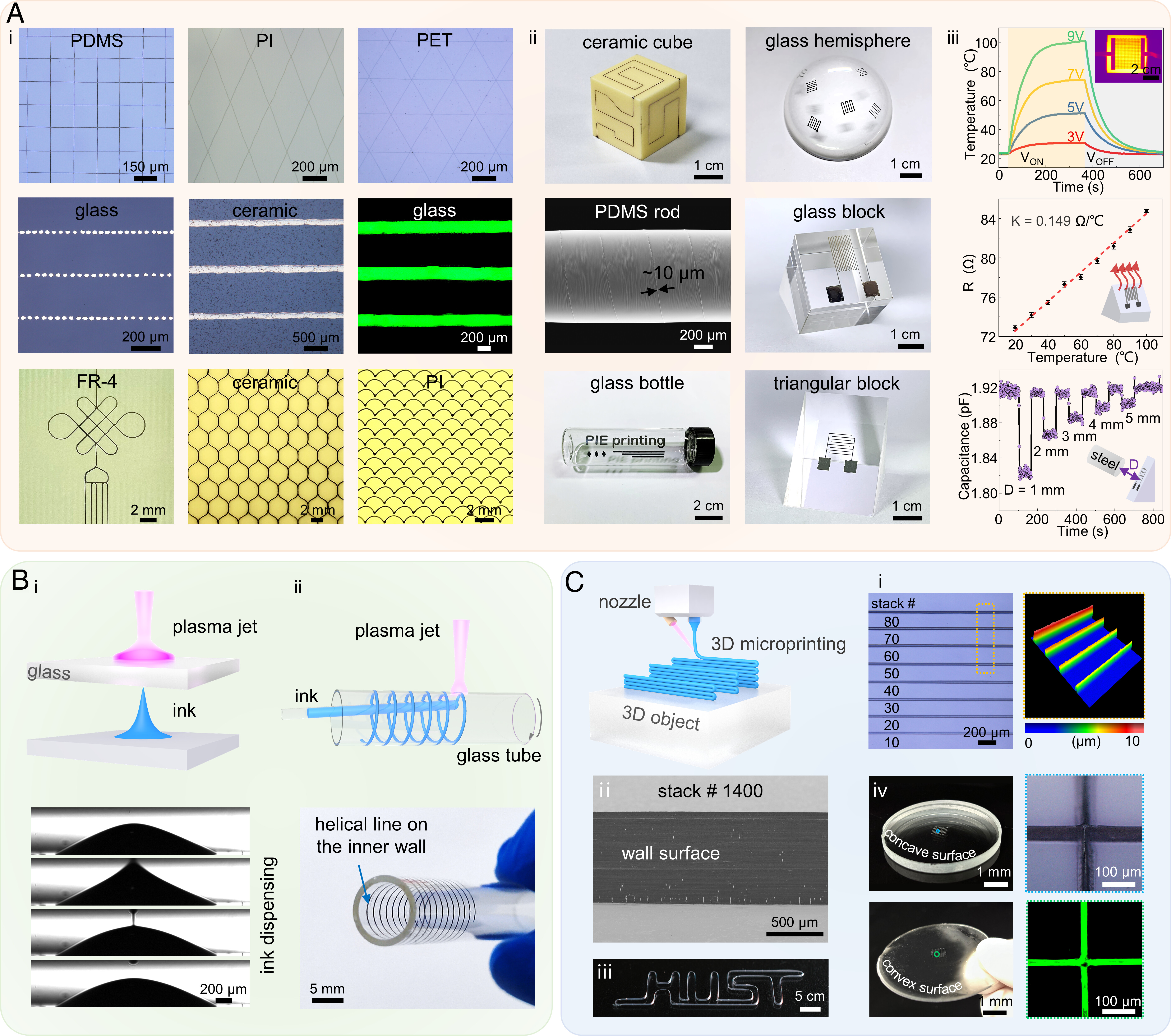
Seamless integration of microstructures and circuits on three-dimensional (3D) complex surfaces is of significance and is catalyzing the emergence of many innovative 3D curvy electronic devices. However, patterning fine features on arbitrary 3D targets remains challenging. Here, we propose a facile charge-driven electrohydrodynamic 3D microprinting technique that allows micron- and even submicron-scale patterning of functional inks on a couple of 3D-shaped dielectrics via an atmospheric-pressure cold plasma jet. Relying on the transient charging of exposed sites arising from the weakly ionized gas jet, the specified charge is programmably deposited onto the surface as a virtual electrode with spatial and time spans of ~mm in diameter and ~μs in duration to generate a localized electric field accordantly. Therefore, inks with a wide range of viscosities can be directly drawn out from micro-orifices and deposited on both two-dimensional (2D) planar and 3D curved surfaces with a curvature radius down to ~1 mm and even on the inner wall of narrow cavities via localized electrostatic attraction, exhibiting a printing resolution of ~450 nm. In addition, several conformal electronic devices were successfully printed on 3D dielectric objects. Self-aligned 3D microprinting, with stacking layers up to 1400, is also achieved due to the electrified surfaces. This microplasma-induced printing technique exhibits great advantages such as ultrahigh resolution, excellent compatibility of inks and substrates, antigravity droplet dispersion, and omnidirectional printing on 3D freeform surfaces. It could provide a promising solution for intimately fabricating electronic devices on arbitrary 3D surfaces.

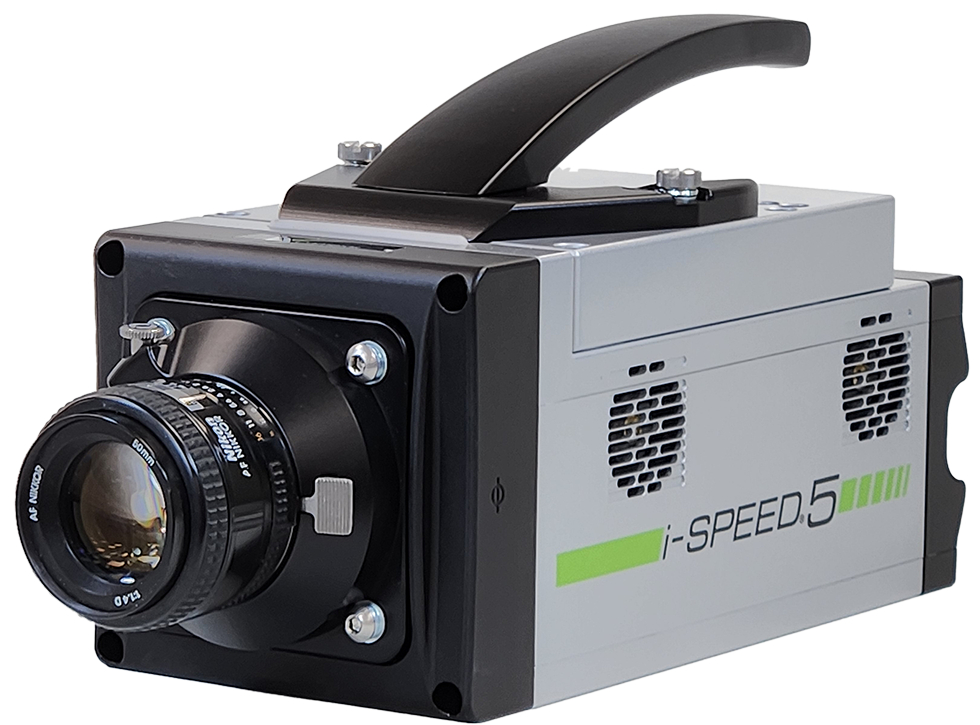
"The highspeed
camera allows for the capture of consecutive pulse cycles, while ICCD cameras need to
prevent overexposure, thus they have limitations in shooting excessive pulse cycles. The reason
for a wider pulse width employed when capturing images with the high-speed camera is that, during
the pulse level phase, the charge density exhibits minor variation, and the adjustment of the pulse
width does not significantly influence the charge distribution or time evolution pattern. Since the
high-speed camera has lower sensitivity compared to ICCD and limited time resolution, a pulse
width of 125 μs (a 25% duty ratio) is adopted to ensure the acquisition of clear data."
